
Two kinds of Wireless
WiFi music streaming is the most popular of it's kind and it works excellent, as long as there is one WiFi receiver. But stereo reproduction from two seperate loudspeakers, each with their own WiFi receiver, is problematic. Now two independent music streams are downloaded to each loudspeaker. This music data needs to be time aligned between the different receivers before it can be used for stereo reproduction. This can only be an approximation and we do not recommend this. Instead, for high quality stereo or even multichannel applications we recommend WiSA wireless. WiSA is different from WiFi streaming. Simply put, WiSA replaces the loudspeaker cable with a dedicated wireless transmitter and receiver. For music streaming, only one WiFi receiver needs to be connected to the WiSA transmitter, thereby eliminating all channel timing issues by definition.


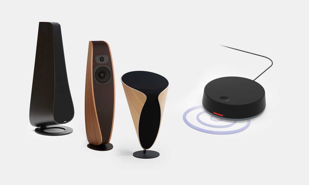
As an alternative we offer using one WiFi receiver for two cabinets for the Twist and Meander, interconnected with a wire. These offer all the benefits of direct streaming of two cabinet stereo, without timing issues.

Davone Wireless DSP Amplifier
Fully developed in-house, our WiSA wireless DSP amplifier transforms the Twist Meander and Solo into superior fully digital wireless loudspeakers. But where the lossless WiSA wireless connection replaces the loudspeaker cable, to us the real benefit lies in the use of a digital crossover. An analog crossover has to abide the laws of physics that dictate, amplitude can only be reduced and that high frequencies always lead the low frequencies when arriving at the listener’s ears.
In our digital crossover however, we delay the higher frequencies to realign them with the lower frequencies. When the music is recombined at your ear, the fundamental of each note and its harmonics arrive perfectly in time, preserving the true character of each instrument. Furthermore, our crossover is implemented in front of the amplfier. It operates at lower voltage and current levels, reducing the tolerances and distortion found in analogue components. And with the ability to make any desired amplitude adjustments needed, our digital crossover is superior to any analog crossover. Compared to analog speakers you will quickly hear more control, more dynamics and more silence.
-
-
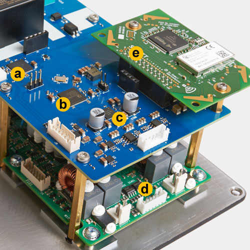
How does it Work?
The Davone module consists of 3 major elements. First, the blue PCB, designed in house, houses the microcontroller (a) which is the brain of the Davone module. It's reliable memory contains all the DSP (b) digital cross over FIR algorithms and many functional tasks like setting the DAC digital filters and temperatur monitoring. The high performance 32 bit Velvet Sound AKM Delta Sigma DAC (c) is handling the conversion to analog. The power is supplied by ultralow noise linear regulators and ample capacitance of different types for a virtual battery like performance. The Low jitter Quartz Crystal Oscillator originates the clocking with a jitter less than 100ps rms.The fully balanced output stage minimises noise and is connected directly to the balanced input of the latest generation ICE power amplifier (d). Last but not least, the audio input to the system is supplied by the WiSA wireless receiver (e). Note the four F shaped antennas on the 4 corners for excellent reception in the 5gHz band.
-
Eye for Detail
High frequency digital signals above 1 MHz, like for example the master clock, need to be routed carefully to maintain high signal integrity. Ideally the connections should be short and direct, but often this is not possible because another signal line crosses it’s path. Textbook four layer print design would divert the trace through a so called via to the bottom layer to cross the obstacle. The second and third layer are used for the ground and power supply planes and therefore already occupied. However, in high frequency circuit design it is vital to keep the distance between the forward and return current traces at a minimum (the path of least inductance). It is therefore much better to route the forward current through the third layer instead of the fourth. That way the return current only has to switch sides on the second layer instead of also jumping planes through one extra via with possible added ground plane noise as a consequence. The improved high frequency current flow is shown in the image above and explained below.
-


-
GET INVOLVED


